- PRODUCTS
- COMPANY
- SUPPORT
- PRODUCTS
- BY TYPE
- BY MARKET
- COMPANY
Our Company
Media
Contact
- SUPPORT
Silicon Photonics Comes of Age
This article is part four in a series on talks delivered at Accelerated Infrastructure for the AI Era, a one-day symposium held by Marvell in April 2024.
Silicon photonics—the technology of manufacturing the hundreds of components required for optical communications with CMOS processes—has been employed to produce coherent optical modules for metro and long-distance communications for years. The increasing bandwidth demands brought on by AI are now opening the door for silicon photonics to come inside data centers to enhance their economics and capabilities.
What’s inside an optical module?
As the previous posts in this series noted, critical semiconductors like digital signal processors (DSPs), transimpedance amplifiers (TIAs) and drivers for producing optical modules have steadily improved in terms of performance and efficiency with each new generation of chips thanks to Moore’s Law and other factors.
The same is not true for optics. Modulators, multiplexers, lenses, waveguides and other devices for managing light impulses have historically been delivered as discrete components.
“Optics pretty much uses piece parts,” said Loi Nguyen, executive vice president and general manager of cloud optics at Marvell. “It is very hard to scale.”
Lasers have been particularly challenging with module developers forced to choose between a wide variety of technologies. Electro-absorption-modulated (EML) lasers are currently the only commercially viable option capable of meeting the 200G per second speed necessary to support AI models. Often used for longer links, EML is the laser of choice for 1.6T optical modules. Not only is fab capacity for EML lasers constrained, but they are also incredibly expensive. Together, these factors make it difficult to scale at the rate needed for AI.
Enter silicon photonics
Unlike traditional optical modules, silicon photonics uses common wavelength (CW) lasers, which are less expensive and easier to make.
“CW is like a lightbulb…It just shines a constant light. It is easier to make and is available from multiple sources and it’s inexpensive,” Nguyen said. “All of the high speed magic for modulating data happens in the silicon photonics.”
Silicon photonics devices can also be produced in 200 or 300 millimeter fabs. For ten years, Marvell has proven that silicon photonics can be manufactured at scale for coherent modules, something that few companies have accomplished.
![]()
The anatomy of a silicon photonics module.
Why silicon photonics now?
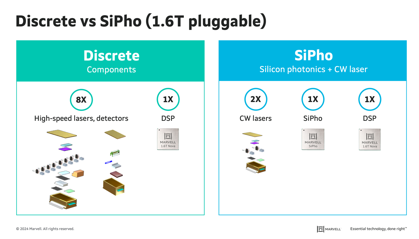
Here's an example: If a discrete module has eight 200G channels in one chip, it requires four EML lasers to run at 1.6T. With silicon photonics, everything is integrated and four channels can share one laser, which means the module only needs two less-expensive CW lasers to run. Integrated silicon photonics modules are also more reliable and scalable.

Silicon photonics modules require fewer, less expensive lasers to deliver the same bandwidth as their discrete counterparts
“Lower cost, fewer lasers and higher integration means more reliability and better scaling,” he added. “When there is a huge pull from the market, integration will always win.”
The future of silicon photonics is here
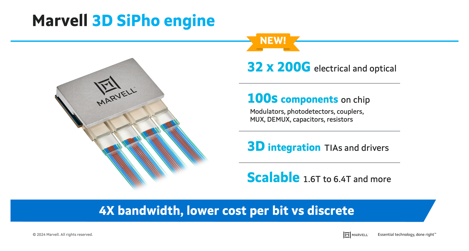
Recently, Marvell announced a live demo of a 6.4T 3D silicon photonics engine with 32 channels that each run at 200G electrical and optical. This engine integrates hundreds of components into the chips, including putting the TIAs and drivers onto the same device. This first-of-its-kind engine is modular, enabling it to scale from 1.6T to 6.4T and beyond. Given the integration, this engine drops the cost per bit compared to discrete solutions and creates a more scalable option to meet ever-increasing bandwidth demand.

The 3D silicon photonics engine will serve as the building block for scaling optics and has multiple use cases across the optical interconnect landscape. The first application will be pluggable optical modules, which will increase the number of channels that can be put into one module from eight to 16, 32, or even 64. In the future, silicon photonics will enable co-packaged optics solutions. Eventually, photonics should find a home in chiplets.
The world will continue to be driven by AI—and interconnect technology must scale to meet demand. By bringing silicon photonics inside the data center, Marvell can continue to deliver the bandwidth needed while increasing scalability and decreasing costs.
# # #
Marvell and the M logo are trademarks of Marvell or its affiliates. Please visit www.marvell.com for a complete list of Marvell trademarks. Other names and brands may be claimed as the property of others.
This blog contains forward-looking statements within the meaning of the federal securities laws that involve risks and uncertainties. Forward-looking statements include, without limitation, any statement that may predict, forecast, indicate or imply future events, results or achievements. Actual events, results or achievements may differ materially from those contemplated in this blog. Forward-looking statements are only predictions and are subject to risks, uncertainties and assumptions that are difficult to predict, including those described in the “Risk Factors” section of our Annual Reports on Form 10-K, Quarterly Reports on Form 10-Q and other documents filed by us from time to time with the SEC. Forward-looking statements speak only as of the date they are made. Readers are cautioned not to put undue reliance on forward-looking statements, and no person assumes any obligation to update or revise any such forward-looking statements, whether as a result of new information, future events or otherwise.
Tags: AI, AI infrastructure, Optical Interconnect, Data Center Interconnects, Data Center Interconnect Solutions, Optical Connectivity, Silicon Photonics, Silicon Photonics Light Engines
Recent Posts
Archives
Categories
- 5G (12)
- AI (30)
- Automotive (26)
- Cloud (16)
- Coherent DSP (10)
- Company News (103)
- Custom Silicon Solutions (7)
- Data Center (55)
- Data Processing Units (22)
- Enterprise (25)
- ESG (6)
- Ethernet Adapters and Controllers (12)
- Ethernet PHYs (4)
- Ethernet Switching (41)
- Fibre Channel (10)
- Marvell Government Solutions (2)
- Networking (36)
- Optical Modules (15)
- Security (6)
- Server Connectivity (26)
- SSD Controllers (6)
- Storage (22)
- Storage Accelerators (2)
- What Makes Marvell (40)
Copyright © 2025 Marvell, All rights reserved.
- Terms of Use
- Privacy Policy
- Contact

