
By Nicola Bramante, Senior Principal Engineer
Transimpedance amplifiers (TIAs) are one of the unsung heroes of the cloud and AI era.
At the recent OFC 2025 event in San Francisco, exhibitors demonstrated the latest progress on 1.6T optical modules featuring Marvell 200G TIAs. Recognized by multiple hyperscalers for its superior performance, Marvell 200G TIAs are becoming a standard component in 200G/lane optical modules for 1.6T deployments.

TIAs capture incoming optical signals from light detectors and transform the underlying data to be transmitted between and used by servers and processors in data centers and scale-up and scale-out networks. Put another way, TIAs allow data to travel from photons to electrons. TIAs also amplify the signals for optical digital signal processors, which filter out noise and preserve signal integrity.
And they are pervasive. Virtually every data link inside a data center longer than three meters includes an optical module (and hence a TIA) at each end. TIAs are critical components of fully retimed optics (FRO), transmit retimed optics (TRO) and linear pluggable optics (LPO), enabling scale-up servers with hundreds of XPUs, active optical cables (AOC), and other emerging technologies, including co-packaged optics (CPO), where TIAs are integrated into optical engines that can sit on the same substrates where switch or XPU ASICs are mounted. TIAs are also essential for long-distance ZR/ZR+ interconnects, which have become the leading solution for connecting data centers and telecom infrastructure. Overall, TIAs are a must have component for any optical interconnect solution and the market for interconnects is expected to triple to $11.5 billion by 2030, according to LightCounting.
By Michael Kanellos, Head of Influencer Relations, Marvell
You’re likely assaulted daily with some zany and unverifiable AI factoid. By 2027, 93% of AI systems will be able to pass the bar, but limit their practice to simple slip and fall cases! Next-generation training models will consume more energy than all Panera outlets combined! etc. etc.
What can you trust? The stats below. Scouring the internet (and leaning heavily on 16 years of employment in the energy industry) I’ve compiled a list of somewhat credible and relevant stats that provide perspective to the energy challenge.
1. First, the Concerning News: Data Center Demand Could Nearly Triple in a Few Years
Lawrence Livermore National Lab and the Department of Energy1 has issued its latest data center power report and it’s ominous.
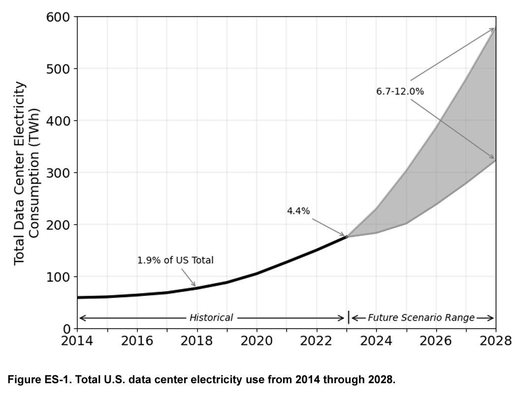
Data center power consumption rose from a stable 60-76 terawatt hours (TWh) per year in the U.S. through 2018 to 176 TWh in 2023, or from 1.9% of total power consumption to 4.4%. By 2028, AI could push it to 6.7%-12%. (Lighting consumes 15%2.)

Report co-author Eric Masanet adds that the total doesn’t include bitcoin, which increases 2023’s consumption by 70 TWh. Add a similar 30-40% to subsequent years too if you want.
This article was originally published in VentureBeat.
Artificial intelligence is about to face some serious growing pains.
Demand for AI services is exploding globally. Unfortunately, so is the challenge of delivering those services in an economical and sustainable manner. AI power demand is forecast to grow by 44.7% annually, a surge that will double data center power consumption to 857 terawatt hours in 20281: as a nation today, that would make data centers the sixth largest consumer of electricity, right behind Japan’s2 consumption. It’s an imbalance that threatens the “smaller, cheaper, faster” mantra that has driven every major trend in technology for the last 50 years.
It also doesn’t have to happen. Custom silicon—unique silicon optimized for specific use cases—is already demonstrating how we can continue to increase performance while cutting power even as Moore’s Law fades into history. Custom may account for 25% of AI accelerators (XPUs) by 20283 and that’s just one category of chips going custom.
The Data Infrastructure is the Computer
Jensen Huang’s vision for AI factories is apt. These coming AI data centers will churn at an unrelenting pace 24/7. And, like manufacturing facilities, their ultimate success or failure for service providers will be determined by operational excellence, the two-word phrase that rules manufacturing. Are we consuming more, or less, energy per token than our competitor? Why is mean time to failure rising? What’s the current operational equipment effectiveness (OEE)? In oil and chemicals, the end products sold to customers are indistinguishable commodities. Where they differ is in process design, leveraging distinct combinations of technologies to squeeze out marginal gains.
The same will occur in AI. Cloud operators already are engaged in differentiating their backbone facilities. Some have adopted optical switching to reduce energy and latency. Others have been more aggressive at developing their own custom CPUs. In 2010, the main difference between a million-square-foot hyperscale data center and a data center inside a regional office was size. Both were built around the same core storage devices, servers and switches. Going forward, diversity will rule, and the operators with the lowest cost, least downtime and ability to roll out new differentiating services and applications will become the favorite of businesses and consumers.
The best infrastructure, in short, will win.
The Custom Concept
And the chief way to differentiate infrastructure will be through custom infrastructure that are enabled by custom semiconductors, i.e., chips containing unique IP or features for achieving leapfrog performance for an application. It’s a spectrum ranging from AI accelerators built around distinct, singular design to a merchant chip containing additional custom IP, cores and firmware to optimize it for a particular software environment. While the focus is now primarily on higher value chips such as AI accelerators, every chip will get customized: Meta, for example, recently unveiled a custom NIC, a relatively unsung chip that connects servers to networks, to reduce the impact of downtime.
By Kirt Zimmer, Head of Social Media Marketing, Marvell
What do you get when you combine some of the world’s leading technology analysts with incredibly smart subject matter experts? Answer: the SixFive Media video podcast. It’s must-view content for anyone interested in understanding exactly how AI technologies are evolving.
At Marvell’s recent Investor Analysts Day, company leaders were happy to chat with Patrick Moorhead, CEO and Chief Analyst at Moor Insights & Strategy, and Daniel Newman, CEO and Chief Analyst at The Futurum Group. The resulting conversations (captured on video) were enlightening:
How Custom HBM is Shaping AI Chip Technology
Fresh off Marvell’s announcement of a partnership with SK Hynix, Micron Technology and Samsung Semiconductor, Patrick and Daniel dove into the details with leaders from those organizations. The partnership centers around custom high bandwidth memory (HBM), which fits inside AI accelerators to store data close to the processors.
Custom designs alleviate the physical and thermal constraints traditionally faced by chip designers by dramatically reducing the size and power consumption of the interface and HBM base die. Marvell estimates that up to 25% of the real estate inside the chip package can be recovered via customization.
Will Chu, SVP and GM of Custom Compute and Storage at Marvell, says the company estimates that the total addressable market (TAM) for data centers in 3-4 years is $75B. Last year it was $21B. Out of that, Marvell estimates that $40-43B is for custom accelerators.
Attached to that is custom HBM, which alleviates bottlenecks for AI workloads. In Dong Kim, VP of Product Planning at Samsung Semiconductor said, “Custom HBM will be the majority portion of the market towards the 2027-28 timeframe.” As Patrick Moorhead said, “The rate of change is phenomenal.”
By Kirt Zimmer, Head of Social Media Marketing, Marvell

Marvell’s business is accelerated infrastructure for the AI era, which is a fast-evolving space that can occasionally confuse even the most earnest student. To help you keep up, we’ve partnered with VentureBeat to explore a multitude of content about that subject: